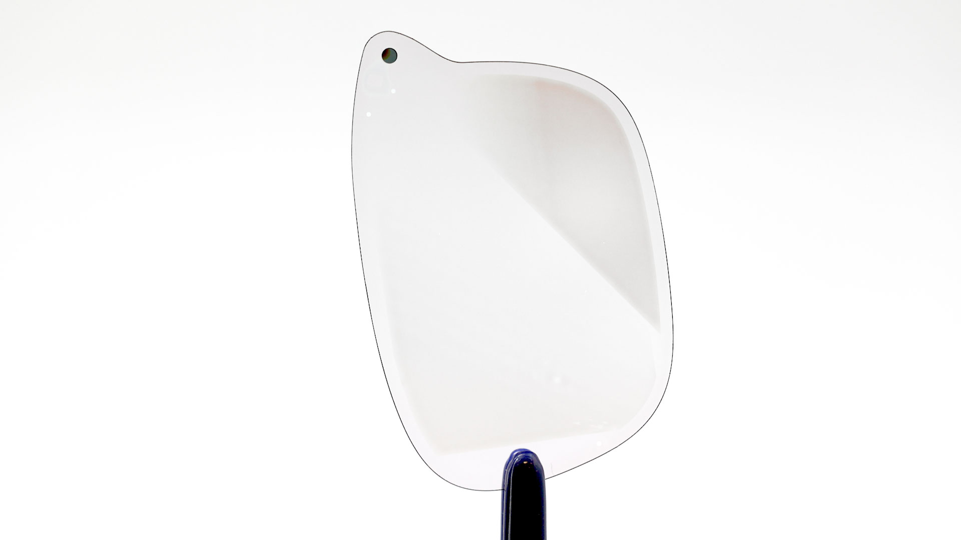
An augmented reality (AR) display must manage two kinds of light at once. Light from the projector must travel through the waveguide and reach the wearer’s eye to form a digital image. Meanwhile, light from the physical world must pass through the waveguide so the wearer can see their surroundings clearly.
Digital content needs to appear bright and consistent, while the view through the waveguide should remain clear, with minimal unwanted reflections or flashes of color. Improving one part of that experience requires understanding how it affects the other, especially for glasses intended to be worn throughout the day.
Our proprietary thin-film optical stack helps us address these requirements together. This stack is a series of extremely thin coatings applied to the waveguide. These carefully engineered layers work with the waveguide’s grating structures to improve see-through quality while preserving and enhancing virtual-image performance.
When Light Meets a Grating
Although far too small to see individually, surface relief gratings control how light moves through the optical system. Light from a projector enters the waveguide through an incoupling grating. It then travels through the waveguide by reflecting between its inner surfaces, a process called total internal reflection, until other gratings direct it toward the wearer’s eye.
The dimensions and arrangement of these structures help determine brightness, color uniformity, efficiency, and field-of-view. They also influence how the waveguide interacts with light from the surrounding environment. Under certain conditions, that interaction can produce multicolored fringes in the wearer’s field-of-view, known as rainbow artifacts.
Grating design plays a central role in controlling these artifacts. Pitch, which is the spacing between repeating grating features, and grating orientation are two design choices that help reduce visible rainbows. The optical layers applied to the waveguide contribute to its broader performance, including how much light passes through and how much is reflected.
These design choices must allow wearers to see their surroundings clearly while viewing digital content through the same optical component.
Designing for TRUE Performance
We design and manufacture waveguides around four primary TRUE key performance metrics: Transmission, Reflection, Uniformity, and Efficiency.
Transmission describes how much light from the physical world passes through the waveguide.
Reflection concerns how much light is reflected away from its surface.
Uniformity describes how consistent the color distribution is across the intended field-of-view.
Efficiency describes the proportion of light generated by the light engine that reaches the wearer’s eye through the waveguide. We evaluate it across each color channel and within the eyebox, the area where the eye can be positioned to view the image. Higher efficiency helps deliver a brighter image from a given amount of projector light.
Our thin-film optical stack is developed with these measures in mind. Its material choices and the arrangement of its layers must work with the grating design to support high transmission, low unwanted reflection, and bright, consistent digital imagery. Reduced rainbow is another important consideration within that broader optical design.
The coatings must also work together. A material that works well on its own may behave differently when combined with other layers or applied over gratings. Each choice therefore has to be evaluated within the complete waveguide.
The stack also serves as a protective hard coat, helping the waveguide withstand handling during manufacturing and assembly, as well as everyday use in AR glasses.
The balance also depends on our partners’ requirements. The projector’s light output, the waveguide’s base material, and the desired field-of-view all influence the optical design. We design the thin-film stack around those requirements.
The Role of Planarization
Planarization is one technique within this broader thin-film approach. It fills the spaces around surface relief gratings with transparent material, producing a smoother surface across the patterned area.
One way to picture it is as filling the valleys in a microscopic landscape. A specially formulated solution is dispensed onto a wafer bearing waveguide grating patterns. Depending on the coating method, an applied force spreads the solution across the surface. Capillary action, which draws liquids into narrow spaces, helps it fill the gaps between the gratings. The process is controlled to achieve the desired coating thickness.
We developed and deployed this thin-film optical architecture to help improve transmission and reduce reflection, with reduced rainbow as a secondary benefit.
We carefully select, test, and validate the coating materials for the waveguide’s intended TRUE performance. By formulating our optical-grade materials in-house, our specialists can continue refining both the materials and the stack’s design. Those refinements support optical performance, handling durability, and the reliability required for production and everyday use.
Expertise Across the Process
Optical simulation helps our engineers predict how materials and layers will affect a waveguide. Physical prototypes and measurements then show how those choices perform when manufactured.
We connect that simulation work with grating design, materials development, metrology, and in-house production. Advanced metrology provides the precise measurements our teams need to assess a waveguide’s physical features and optical performance. Our teams can adjust a formulation, apply it to wafers bearing gratings, evaluate the results, and use those findings to guide further improvements.
Reliability testing helps us evaluate how optical materials perform over time and under different environmental conditions. By developing and testing these materials in-house, we can refine their transparency, durability, and optical properties together.
Over 15 years of pioneering work and continued optical development, we have built a detailed understanding of how materials, grating structures, and manufacturing processes work together. That knowledge guides our teams as they develop optical layers around each partner’s performance requirements.
For partners, that means we can connect optical requirements with practical development and manufacturing decisions. We can adapt established materials and processes, test proposed changes in prototypes, and assess their effect on both see-through quality and digital-image performance. Those capabilities help us develop waveguides suited to the AR devices our partners are building.
Explore how we combine our materials expertise with waveguide design and advanced manufacturing to help our partners develop production-ready AR solutions.