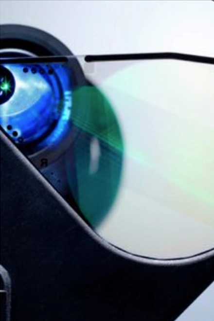
Waveguides

Our industry-leading waveguide technology delivers precise digital content overlayed on top of the physical world.

Waveguides
The heart of the optics stack
Protected between two ultra-thin lenses, the waveguide is a transparent display that controls light in such a way that we can overlay digital content on top of the physical world. We have the technology, experience, and intellectual property to flex device field-of-view from 20° to 70°.
Over the past 10 years, we’ve developed innovative ways to design thinner, more efficient, and powerful waveguide solutions. Our patented nano-imprint process has resulted in lighter waveguides with outstanding visual comfort and versatility.
Magic Leap designs advanced waveguide optics compatible with all major light engine architectures, including LCoS, micro-LED, and laser-illuminated light engines, without locking our partners into a single approach.
Waveguide Innovation
Custom design and development

We use high-performance materials and custom machinery to develop industry-leading waveguides.
From ideation and rigorous testing to finalized prototypes, our design process is focused on human comfort, wearability, and scalability.
Our proprietary Jet and Flash Imprint Lithography (J-FIL) and Lithoflex processes deliver waveguides with greater performance and value that are adaptable to partner product specifications. We offer various field-of-view configurations and can engage with partners on customized approaches to align performance with specific product objectives.
Waveguide Design
Simulation-Driven Design
Prototyping
Material Science Expertise
Human-Centered Metrics
Field-of-View
Form and function
We have the technology, experience, and intellectual property to flex device FOV from 20° to 70°, depending on the form factor.
Our advanced optics technologies and eyepiece designs enable precise content placement so users have the best experience, with minimal distraction and visual fatigue.
Production-Ready
Redefining waveguide fabrication
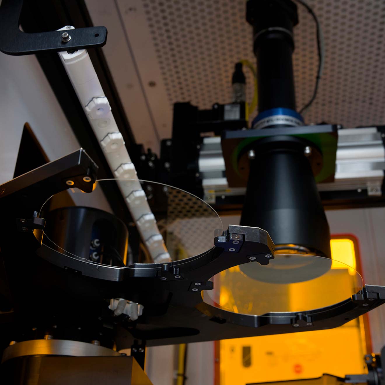
Our proprietary Jet and Flash Imprint Lithography (J-FIL) unlocks single-step patterning with precise depth gradation to deliver scalable, high-yield manufacturing for waveguides. Unlike conventional lithography and multi-cycle 2D etching, J-FIL creates complex 3D structures in one step, combining speed with precision. With cross-disciplinary expertise spanning fabrication, materials, and process engineering, we streamline production without sacrificing optical precision.
Manufacturing Insights
Single-Step Imprinting
Production-Grade Materials
Metrology and Testing
Manufacturing at Scale

Waveguide Offerings
Our waveguide samples are available in a variety of field-of-view options to support diverse use cases.
Connect with us at care@magicleap.com to learn more about our waveguides.