
Developing a waveguide involves a lot of moving parts. Design decisions can affect materials, testing can uncover changes needed during manufacturing, and adjustments in one area can create new considerations elsewhere in the process.
Keeping these capabilities closely connected can make that process easier to manage. With in-house expertise and on-site tools and facilities, our teams can share information, make adjustments, and move a waveguide toward production without relying on a network of separate suppliers for each step.
The Vertical Integration Advantage
While an alliance of multiple vendors may bring together the right simulation, calibration, materials, fabrication, and metrology capabilities, coordinating them can get complicated. Every step requires another handoff, another conversation, and another opportunity for information to get lost or misinterpreted along the way. This can slow feedback and make it harder to respond when a design needs to change.
Our teams work as one, with our people, equipment, and technical expertise at one facility. This matters because waveguide development is iterative, with teams continually building, testing, and refining designs based on what they learn.
By sharing the same workflows and communication channels, we can coordinate directly, exchange feedback quickly, and make adjustments without the delays typical of working across multiple companies. This creates a more streamlined way to design, build, and test waveguides.
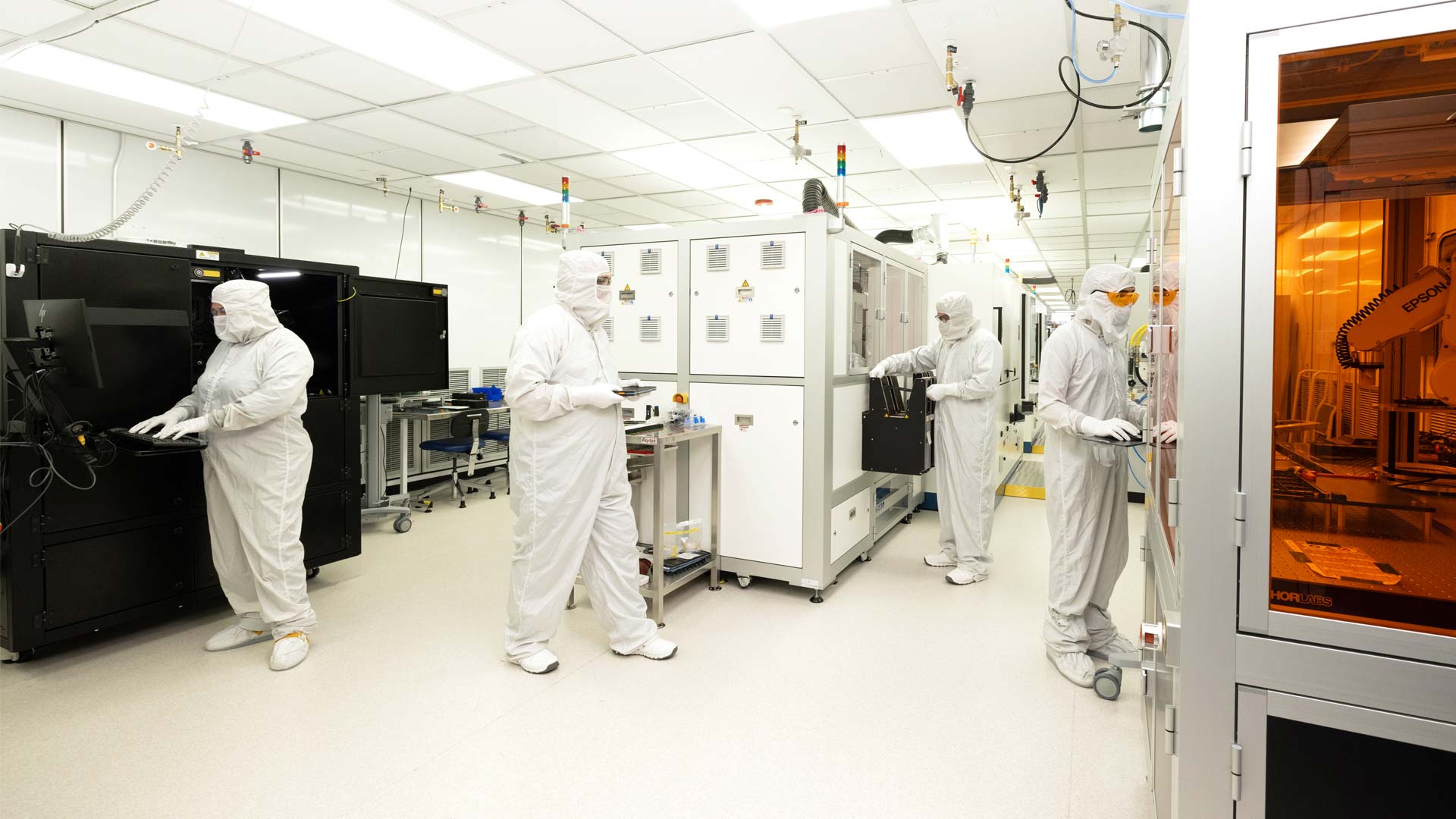
Vertical Integration in Action
Having teams and capabilities in one place changes how quickly we can put ideas into practice. Instead of waiting for work or information to move between suppliers, our teams can use what they learn to inform what happens next.
Faster Testing and Iteration
Having development and testing capabilities on site allows our teams to test ideas and respond to what they learn.
By turning customer specifications into fast, iterative simulations, our waveguide design group works hand-in-hand with our materials, front-end, and back-end process engineering teams. Rapid waveguide prototyping and optical testing feed critical performance data directly back into design, ensuring we lock in final build specifications quickly and accurately.
Keeping this work in-house shortens feedback loops and helps ensure that builds move forward without third-party delays.
Reduced Costs
Time spent in development is often the most expensive component of bringing a waveguide to production. Handoffs between multiple parties create delays and introduce communication gaps that frequently lead to misaligned specifications, wasted resources, and costly redesigns.
Bringing waveguide design, prototyping, testing, and manufacturing under one roof means we eliminate multi-company friction. Direct, real-time collaboration allows us to catch edge cases early and refine designs immediately. The result is a streamlined development cycle that protects time to market, conserves engineering resources, and helps waveguides reach production faster.
Learn how we approach integrated waveguide manufacturing.